A Low-Frequency Crystal Controlled Oscillator
Ing. Ramón Vargas Patrón
INICTEL
The RF engineer sometimes has to look for an instrument that will check a low frequency quartz crystal unit reliably and rapidly. This is a difficult piece of equipment to find and the engineer often has to consult an electronic circuits handbook for the schematic of a circuit that will perform the task.
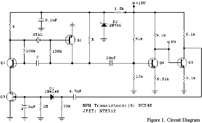
Unfortunately, there aren't many such circuits in the technical literature currently available, and when found, they don't always work as expected. A circuit that has been found to work at full satisfaction in the frequency range from 10 kHz to 500 kHz is illustrated in Figure 1.
This is a schematic of a low frequency sine wave oscillator featuring low distortion, wide-band operation and crystal control. The circuit, originally developed for laboratory use, employs low cost AF bipolar transistors for the oscillator and amplifier sections and a JFET for loop-gain control. Operation of the oscillator in the 10 kHz to 500 kHz frequency range has been found to be excellent, while measured distortion is kept under 0.1 percent
Theory of Operation
Q1, Q2 and associated circuitry form a modified astable multivibrator in which the loop gain is automatically adjusted to the threshold of oscillation by means of field effect transistor Q3. Q4 linearly amplifies the signal present at the collector of Q2 and isolates the oscillator section of the circuit from the output.
This stage features wide-band operation and delivers a clean 2.5 Volt amplitude sine wave into a resistive load greater than or equal to 20k Ohms. The stage comprising Q5 has a voltage gain of 1 and its sole purpose is to isolate the non-linear effects of rectifier D1 from the output. Transistor Q4 also amplifies the minor changes in amplitude of the oscillator's waveform due to temperature effects and/or power supply variations, so a magnified version of the perturbance is fed back to rectifier D1 producing a corresponding change in Q3's gate voltage. This action modifies the FET's drain-source resistance and hence adjusts the loop gain to a new value slightly above unity, just enough to maintain a constant amplitude in the output.
Experimental Results
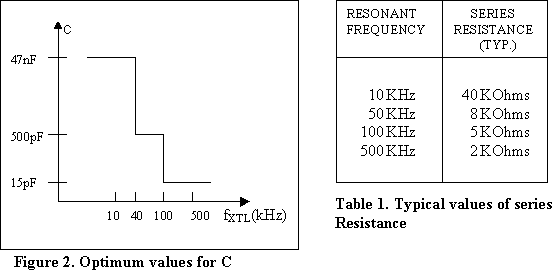
Figure 2 shows optimum values for capacitor C according to the crystal's resonant frequency. Extra gain is needed from transistors Q1 and Q2 at frequencies below 40 kHz. This is due to the fact that low frequency crystals exhibit large values of series resistance, affecting loop gain (Table 1 compares typical values of series resistance for low frequency units). According to what has been stated, resistor R is made 10k Ohms for frequencies under 40 kHz. Above this value, 1K Ohm will do.
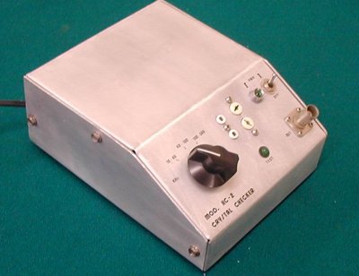
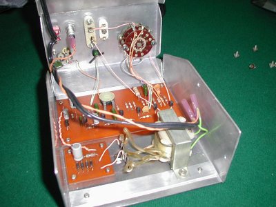
NOTE: The photographs show a lab instrument based on the circuit discussed. A panel lamp glows when the circuit is oscillating, indicating that the crystal being tested is in a good condition. Furthermore, a BNC connector permits checking of the waveform's frequency. Crystal range can be selected by means of a three-way switch, i.e., 10 ~ 40 kHz, 40 ~ 100 kHz and 100 ~ 500 kHz. Two different sockets are available for the crystal.
References